CZ:Featured article/Current: Difference between revisions
imported>Chunbum Park mNo edit summary |
imported>Chunbum Park No edit summary |
||
| Line 1: | Line 1: | ||
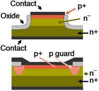
{{Image|Two diode structures.PNG|right|200px|Mesa diode structure (top) and planar diode structure with guard-ring (bottom).}} | |||
A '''[[semiconductor diode]]''' is a two-terminal device that conducts current in only one direction, made of two or more layers of which at least one is a semiconductor. An example is the ''pn''-diode, made by joining a ''p''-type semiconducting layer to an ''n''-type semiconducting layer. For a discussion of dopant impurities and the terminology ''p-'' and ''n-''type. see [[Semiconductor#Dopant_impurities|dopant impurities]]. | |||
The | The figure shows two of the many possible structures used for ''pn-''semiconductor diodes, both adapted to increase the voltage the devices can withstand in reverse bias. The top structure uses a mesa to avoid a sharp curvature of the ''p<sup>+</sup>-''region next to the adjoining ''n-''layer. The bottom structure uses a lightly doped ''p-''guard-ring at the edge of the sharp corner of the ''p<sup>+</sup>-''layer to spread the voltage out over a larger distance and reduce the electric field. (Superscripts like ''n<sup>+</sup>'' or ''n<sup>−</sup>'' refer to heavier or lighter impurity doping levels.) | ||
==Types== | |||
Semiconductor diodes come in a large variety of types: | |||
*''pn''-diode: The ''pn'' junction diode consists of an ''n''-type semiconductor joined to a ''p''-type semiconductor. | |||
*Zener diode: The Zener diode is a special type of ''pn''-diode made to operate in the reverse breakdown region, and used often as a voltage regulator. The breakdown voltage in these diodes is sometimes called the ''Zener voltage''. Depending upon the voltage range designed for, the diode may break down by either Zener breakdown, an electron tunneling behavior, or by avalanche breakdown. | |||
*Schottky diode: The Schottky diode is made using a metal such as aluminum or platinum, on a lightly doped semiconductor substrate. | |||
*Tunnel diode: Like the Zener diode, the tunnel diode (or Esaki diode) is made up of heavily doped ''n-'' and ''p''-type layers with a very abrupt transition between the two types. Conduction takes place by electron tunneling. | |||
*Light-emitting diode: The light-emitting diode is designed to convert electrical current into light. | |||
*Photodiode: The photodiode is the inverse of the light-emitting diode, acting as a photodetector, converting incident light to a detectable electric current. | |||
*''pin''-diode: The ''pin''-diode is made of three layers: an intrinsic (undoped) layer between the ''p''- and ''n''-type layers. Because of its rapid switching characteristics it is used in microwave and radio-frequency applications. | |||
*Gunn diode: The Gunn diode is a ''transferred electron device'' based upon the Gunn effect in III-V semiconductors, and is used to generate microwave oscillations. | |||
*Varactor: a ''pn''-junction used in reverse bias as a voltage-variable capacitor for tuning radio receivers. The term ''varactor'' also is used for devices that behave like back-to-back Zener diodes. | |||
[[semiconductor diode|...]] | |||
[[ | |||
Revision as of 12:24, 17 June 2011
A semiconductor diode is a two-terminal device that conducts current in only one direction, made of two or more layers of which at least one is a semiconductor. An example is the pn-diode, made by joining a p-type semiconducting layer to an n-type semiconducting layer. For a discussion of dopant impurities and the terminology p- and n-type. see dopant impurities.
The figure shows two of the many possible structures used for pn-semiconductor diodes, both adapted to increase the voltage the devices can withstand in reverse bias. The top structure uses a mesa to avoid a sharp curvature of the p+-region next to the adjoining n-layer. The bottom structure uses a lightly doped p-guard-ring at the edge of the sharp corner of the p+-layer to spread the voltage out over a larger distance and reduce the electric field. (Superscripts like n+ or n− refer to heavier or lighter impurity doping levels.)
Types
Semiconductor diodes come in a large variety of types:
- pn-diode: The pn junction diode consists of an n-type semiconductor joined to a p-type semiconductor.
- Zener diode: The Zener diode is a special type of pn-diode made to operate in the reverse breakdown region, and used often as a voltage regulator. The breakdown voltage in these diodes is sometimes called the Zener voltage. Depending upon the voltage range designed for, the diode may break down by either Zener breakdown, an electron tunneling behavior, or by avalanche breakdown.
- Schottky diode: The Schottky diode is made using a metal such as aluminum or platinum, on a lightly doped semiconductor substrate.
- Tunnel diode: Like the Zener diode, the tunnel diode (or Esaki diode) is made up of heavily doped n- and p-type layers with a very abrupt transition between the two types. Conduction takes place by electron tunneling.
- Light-emitting diode: The light-emitting diode is designed to convert electrical current into light.
- Photodiode: The photodiode is the inverse of the light-emitting diode, acting as a photodetector, converting incident light to a detectable electric current.
- pin-diode: The pin-diode is made of three layers: an intrinsic (undoped) layer between the p- and n-type layers. Because of its rapid switching characteristics it is used in microwave and radio-frequency applications.
- Gunn diode: The Gunn diode is a transferred electron device based upon the Gunn effect in III-V semiconductors, and is used to generate microwave oscillations.
- Varactor: a pn-junction used in reverse bias as a voltage-variable capacitor for tuning radio receivers. The term varactor also is used for devices that behave like back-to-back Zener diodes.
