User:John R. Brews/WP Import
The hybrid-pi model is a popular circuit model used for analyzing the small signal behavior of transistors. The model can be quite accurate for low-frequency circuits and can easily be adapted for higher frequency circuits with the addition of appropriate inter-electrode capacitances and other parasitic elements.
Bipolar transistor
The hybrid-pi model is a linearized, y-parameter two-port network approximation to the transistor using the small-signal base-emitter voltage vπ and collector-emitter voltage vce as independent variables, and the small-signal base current ib and collector current ic as dependent variables. (See Jaeger and Blalock.[1])
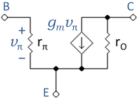
A basic, low-frequency hybrid-pi model for the bipolar transistor is shown in the figure. The three transistor terminals are E = emitter, B = base, and C = collector. The base-emitter connection is through a resistor rπ, and the base current causes a small-signal voltage drop across it, vπ (the π notation is standard). Voltage vπ induces a small-signal collector current via the voltage-controlled current source with current gmvπ, gm is the transistor transconductance.
The various parameters are as follows.
- is the transconductance in siemens, evaluated in a simple model (see Jaeger and Blalock[2])
- where:
- is the quiescent collector current (also called the collector bias or DC collector current)
- is the thermal voltage, calculated from Boltzmann's constant, the charge on an electron, and the transistor temperature in kelvins. At 290 K (an approximation to room temperature: 70°F ≈ 294 K) VT is very nearly 25 mV (Google calculator).
- in ohms
- where:
- is the current gain at low frequencies (commonly called hFE). Here is the Q-point base current. This is a parameter specific to each transistor, and can be found on a datasheet; is a function of the choice of collector current.
- is the output resistance due to the Early effect.
Higher frequencies
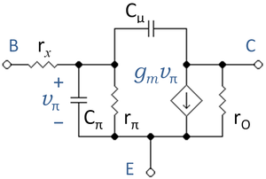
As frequencies are increased, amplifier gain drops off with increasing frequency. as the bipolar transistor is degraded by parasitic capacitances. These effects must be modeled to assess the limitations of bipolar circuits. Three parasitic elements are commonly added to the hybrid-pi model to make frequency predictions. One is the base-emitter capacitance Cπ, which includes the base-emitter diffusion capacitance and the base-emitter junction capacitance. At high enough frequencies, Cπ shorts out the transistor and it fails to function. A second parasitic capacitance Cμ connects the base to the collector. Although this capacitor is small, its influence is multiplied by the transistor gain which amplifies the voltage variation at the base connection and applies it to the collector connection, exaggerating the influence of this capacitor through the Miller effect. The small series base resistance rx plays a role only when there is no other resistance introduced by the circuit into the base lead.
Related terms
The reciprocal of the output resistance is named the output conductance
- .
The reciprocal of gm is called the intrinsic resistance
- .
MOSFET parameters

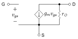
A basic, low-frequency hybrid-pi model for the MOSFET is shown in figure 2. The various parameters are as follows.
is the transconductance in siemens, evaluated in the Shichman-Hodges model in terms of the Q-point drain current by (see Jaeger and Blalock[3]):
- ,
- where:
- is the quiescent drain current (also called the drain bias or DC drain current)
- = threshold voltage and = gate-to-source voltage.
The combination:
often is called the overdrive voltage.
- is the output resistance due to channel length modulation, calculated using the Shichman-Hodges model as
- ,
using the approximation for the channel length modulation parameter λ[4]
- .
Here VE is a technology related parameter (about 4 V / μm for the 65 nm technology node[4]) and L is the length of the source-to-drain separation.
The reciprocal of the output resistance is named the drain conductance
- .
References and notes
- ↑ R.C. Jaeger and T.N. Blalock (2004). Microelectronic Circuit Design, Second Edition. New York: McGraw-Hill, Section 13.5, esp. Eqs. 13.19. ISBN 0-07-232099-0.
- ↑ R.C. Jaeger and T.N. Blalock. Eq. 5.45 pp. 242 and Eq. 13.25 p. 682. ISBN 0-07-232099-0.
- ↑ R.C. Jaeger and T.N. Blalock. Eq. 4.20 pp. 155 and Eq. 13.74 p. 702. ISBN 0-07-232099-0.
- ↑ 4.0 4.1 W. M. C. Sansen (2006). Analog Design Essentials. Dordrechtμ: Springer. ISBN 0-387-25746-2.


