Nullor
In electronics, a nullor is a theoretical two-port network composed of a nullator at its input and a norator at its output.[1] Nullors represent an ideal amplifier, having infinite current, voltage, transconductance and transimpedance gain.[2] Its transmission parameters are all zero, that is, its input-output behavior is summarized with the matrix:
- Failed to parse (SVG (MathML can be enabled via browser plugin): Invalid response ("Math extension cannot connect to Restbase.") from server "https://wikimedia.org/api/rest_v1/":): {\displaystyle \begin{pmatrix} v_i\\ i_i \end{pmatrix} = \begin{pmatrix} 0 & 0 \\ 0 & 0 \end{pmatrix} \begin{pmatrix} v_o\\ i_o \end{pmatrix} \ . }
That is, any non-zero input vi, ii leads to infinite output vo, io. Consequently the nullor makes sense only in a feedback network. In negative feedback circuits, the circuit surrounding the nullor determines the nullor output in such a way as to force the nullor input to zero.
Inserting a nullor in a circuit schematic imposes mathematical constraints on how that circuit must behave, forcing the circuit itself to adopt whatever arrangements are needed to meet the conditions. For example, an ideal op amp can be modeled using a nullor,[3] and the textbook analysis of a feedback circuit using an ideal op amp uses the mathematical conditions imposed by the nullor to analyze the circuit surrounding the op amp.
Example: voltage-controlled current sink
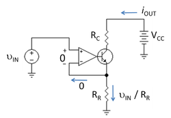
The figure shows a voltage-controlled current sink.[4] The sink is intended to draw the same current iOUT regardless of the applied voltage VCC at the output. The value of current drawn is to be set by the input voltage vIN. Here the sink is to be analyzed by idealizing the op amp as a nullor.
Using properties of the input nullator portion of the nullor, the input voltage across the op amp input terminals is zero. Consequently, the voltage across reference resistor RR is the applied voltage vIN, making the current in RR simply vIN / RR. Again using the nullator properties, the input current to the nullor is zero. Consequently, Kirchhoff's current law at the emitter provides an emitter current of vIN / RR. Using properties of the norator output portion of the nullor, the nullor provides whatever current is demanded of it, regardless of the voltage at its output. In this case, it provides the transistor base current iB. Thus, Kirchhoff's current law applied to the transistor as a whole provides the output current drawn through resistor RC as:
- Failed to parse (SVG (MathML can be enabled via browser plugin): Invalid response ("Math extension cannot connect to Restbase.") from server "https://wikimedia.org/api/rest_v1/":): {\displaystyle i_{OUT} = \frac {v_{IN}} {R_{R}} -i_B \ , }
where the base current of the bipolar transistor iB is normally negligible provided the transistor remains in active mode. That is, based upon the idealization of a nullor, the output current is controlled by the user-applied input voltage vIN and the designer's choice for the reference resistor RR.
The purpose of the transistor in the circuit is to reduce the portion of the current in RR supplied by the op amp. Without the transistor, the current through RC would be iOUT = ( VCC − vIN ) / RC, which interferes with the design goal of independence of iOUT from VCC. Another practical advantage of the transistor is that the op amp must deliver only the small transistor base current, which is unlikely to tax the op amp's current delivery capability. Of course, only real op amps are current-limited, not nullors.
The remaining variation of the current with the voltage VCC is due to the Early effect, which causes the β of the transistor to change with its collector-to-base voltage VCB according to the relation β = β0 ( 1 + VCB / VA ), where VA is the so-called Early voltage. Analysis based upon a nullor leads to the output resistance of this current sink as Rout = rO ( β + 1 ) + RC , where rO is the small-signal transistor output resistance given by rO = ( VA + VCB ) / iout. See current mirror for the analysis.
Use of the nullor idealization allows design of the circuitry around the op amp. The practical problem remains of designing an op amp that behaves like a nullor.
References
- ↑ The name "nullor" was introduced by H.J. Carlin (March 1965). "Singular network elements" CT-11: pp. 67-72. DOI:10.1109/TCT.1964.1082264. Research Blogging.
- ↑ Verhoeven C J M van Staveren A Monna G L E Kouwenhoven M H L & Yildiz E (2003). “§2.2.2: The nullor”, Structured electronic design: negative feedback amplifiers. Boston/Dordrecht/London: Kluwer Academic, pp. 32–34. ISBN 1402075901.
- ↑ Verhoeven C J M van Staveren A Monna G L E Kouwenhoven M H L & Yildiz E. “§2.6.2: Two-ports with active devices”, Cited work, pp. 41 ff. ISBN 1402075901.
- ↑ Richard R Spencer & Ghausi MS (2003). Introduction to electronic circuit design. Upper Saddle River NJ: Prentice Hall/Pearson Education, §5.1.6 pp. 226–227. ISBN 0-201-36183-3.
