Transistor

In electronics, a transistor is a semiconductor device that allows a signal at its input terminal(s) (usually a current or a voltage) to control an output signal at its output terminal(s), acting either as a switch activated by the input signal or as an amplifier for the input signal. Transistors are much smaller than vacuum tubes but perform most of the same functions. As transistors became viable commercially in the 1960's and later, much smaller sizes were possible for the electronics used in computers, radios and televisions. Over time, transistors also led to higher reliability by avoiding the relatively high failure rates of vacuum tubes.
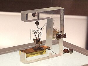
The first transister was built by John Bardeen, William Shockley and Walter H. Brattain at Bell Laboratories in 1947, for which they received the Nobel Prize in Physics in 1956.
The most common transistors are the three-terminal bipolar transistor and the four-terminal Metal-oxide-semiconductor field-effect transistor or MOSFET.
Bipolar junction transistor

A planar bipolar junction transistor as might be constructed in a integrated circuit.
A planar bipolar transistor is shown in the figure. The input terminal may be any of the three contacts and the output is connected to the other two. In a common emitter circuit, the emitter (E) is common to input and output, while the signal is applied to the base (B) and the collector (C) is part of the output circuit. Other circuit arrangements make either the collector or the base common to both the input and output.
In the figure, the labels p, n, p+, n+ refer to dopant impurities, with p referring to dopants that introduce positive charge carriers (holes) and n to dopants that introduce negative charge carriers (electrons). The superscript '+' indicates heavy doping.
For more detail see the articles bipolar transistor and semiconductor.
MOSFET
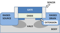
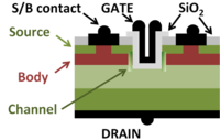
The figures show two example MOSFETs. The input terminals are usually the gate and source contacts, and the output terminals at the source and drain contacts. In many applications, the source and body contacts are short-circuited, making a three-terminal device. However, as for the bipolar transistor, some circuits use different input and output contacts.
For more detail see the article MOSFET.

